Lowered threshold for 3D printing of electronics
Shorter development and delivery cycles will become the biggest challenge for the electronics industry
To accelerate the application of 3D printed electronics, Nano Dimension and the German Hensoldt are starting a joint venture. In addition to creating a platform to share knowledge, experiences and designs, an open prototype lab is being built in Germany. Smaller companies can also use the Dragonfly 3D printer use here.
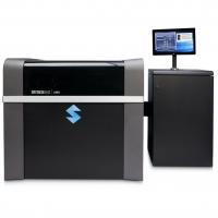
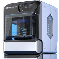
Hensoldt is one of the leading players in the global defense and cybersecurity industry. It is one of the pioneers when it comes to 3D printing of electronics, Additively Manufactured Electronics (AME). With the AME systems from Nano Dimension 3D, the German company prints the electronic components directly from the design software. No tooling is required for this, nor are there any minimum purchase quantities.

Yoav Stern (left) from Nano Dimension together with Thomas Müller, CEO of Hensoldt.
Investment of $6 million
Both companies are jointly investing $6 million in the joint venture. This goes under the name J. A. M. E. S. Operate: Jetted Additively Manufactures Electronics Sources, referring to the Israeli company's 3D printing technology. J. A. M. E. S. Is located in Taufkirchen, near Munich. The joint venture first offers a cloud platform. This platform connects the entire value chain of designers and users of printed electronics. This creates an international community for designers and users in which they can share knowledge of materials, production techniques and designs with each other. In addition, the joint venture will have access to a production laboratory in Taufkirchen. This is where the Dragonfly electronics printer is located Nano Dimension . By offering the printing facility, community members can immediately convert their ideas into a physical prototype or product.
Accelerate
“We expect that the closer collaboration with Nano Dimension will accelerate both development cycles and production of spare parts,” said Marian Rachow, head of Hensoldt Ventures, Hensoldt's investment arm. Hensoldt has now gained a lot of experience with 3D printing of electronics. It is the first in the world to produce a 10-layer PCB on a Dragonfly 3D printer. “Increasing competition and shorter delivery cycles will pose one of the biggest challenges for established suppliers in the future. Our joint venture, J. A. M. E. S, not only offers rapid development of the technology as a real alternative to conventional electronics manufacturing, but also offers small and medium-sized enterprises the opportunity to efficiently design new products.”

Ecosystem for AME
Yoav Stern, CEO of Nano Dimension and Chairman of J. A. M. E. S. Sees the joint venture as a building block for a powerful ecosystem for printed electronics. “We think that in the future, companies will upload a wide variety of electronics components into their usual CAD/CAM/CAE software and convert them on the platform into a new type of AME file. Adjustments can be made via the platform, possibly changing the shape, after which the components will be printed on-demand.”

Over 20 years of experience
Experience, expertise, and customer satisfaction are the cornerstones of our company.

Authorized distributor
Your AM partner in the Benelux, France, and the Nordics, with service operations and local offices in each region.

Go for the best deal
We offer a range of financing options to suit every use case, including renting, leasing, and trade-in solutions.